Figure
1.
RX block diagram of the hybrid phased array system.
| Citation: |
Dingyuan Zeng, Haoshen Zhu, Outong Gao, et al., “A k/ka-band frequency reconfigurable gan LNA for multi-band communication applications,” Chinese Journal of Electronics, vol. x, no. x, pp. 1–10, xxxx. DOI: 10.23919/cje.2024.00.149

|
 Zeng Dingyuan: Dingyuan Zeng received the B.S. degree in communication engineering from the Guangdong University of Technology (GDUT), Guangzhou, China, in 2018, and the M.Eng. degree in Integrated Circuit Engineering from the South China University of Technology (SCUT), Guangzhou, in 2021, where he is currently pursuing the Ph.D. degree. His current research interests include III-V RF/millimeter-wave integrated circuits design. (Email: ee_tingyuen@mail.scut.edu.cn)
 Zhu Haoshen: Haoshen Zhu received the B.E. degree in electrical engineering from the Wuhan University of Technology, Wuhan, China, in 2009, and the Ph.D. degree in electronics engineering from the City University of Hong Kong, Hong Kong, in 2015. His research interests include RF MEMS devices, integrated circuits and microsystems for RF, timing, and sensing applications. (Email: zhuhs@scut.edu.cn)
 Gao Outong: Outong Gao received her M.Eng. degree in Integrated Circuit Engineering from South China University of Technology in 2023. She is pursuing her PhD degree in Electronics and Computer Engineering (ECE) department, The Hong Kong University of Science and Technology, Hong Kong. Her current research focuses on mmWave RFFE design. (Email: sheryl_0114@foxmail.com)
 Cai Zongqi: Zongqi Cai received the Ph.D. degrees in the school of electronic science and engineering from UESTC, Chengdu, China, in 2020. His research interests include the design and measurement of RF/microwave low phase noise oscillator/amplifier/filter/Doppler radar and also the electromagnetic compatibility, failure analysis, and reliability of microwave components and circuits. (Email: zqcai.uestc@hotmail.com)
 Che Wenquan: Wenquan Che received the B.Sc. degree from the East China Institute of Science and Technology, Nanjing, China, in 1990, the M.Sc. degree from the Nanjing University of Science and Technology (NUST), Nanjing, in 1995, and the Ph.D. degree from the City University of Hong Kong (CITYU), Kowloon, Hong Kong, in 2003. Her research interests include electromagnetic computation, planar/coplanar circuits and subsystems in RF/microwave frequency, microwave monolithic integrated circuits (MMICs), and medical application of microwave technology. (Email: eewqche@scut.edu.cn)
 Xue Quan: Quan Xue received the B.Sc., M.Sc., and Ph.D. degrees in electronic engineering from the University of Electronic Science and Technology of China (UESTC), Chengdu, China, in 1988, 1991, and 1993, respectively. His research interests include microwave/millimeter-wave/THz passive components, active components, antenna, and microwave monolithic integrated circuits (MMIC) and radio frequency integrated circuits (RFIC). (Email: eeqxue@scut.edu.cn)
A frequency reconfigurable low noise amplifier (LNA) in a 0.15-μm GaN HEMT process. The frequency reconfiguration concept of utilizing a switch-based reconfigurable resonator (SBRR) to adjust the resonant frequency and introduce a transmission zero in the lower out-of-band region is presented. Additionally, a K/Ka-band frequency-reconfigurable LNA that incorporates the SBRR is designed and fabricated for validation. The proposed LNA features a small-signal gain of 13.9/8.9 dB and an NF of 2.4/3.2 dB at 21/30 GHz. The measured output power 1-dB compression point (OP1dB) is 5.5/6.7 dBm at 21/30 GHz, respectively. The chip size is 1.5×1.75 mm2. The reconfigurable GaN LNA is attractive for future multi-band communication systems compatible for multiple standards.
Advancements in satellite communication (SATCOM) technology have significantly improved latency and capacity for global internet access compared to conventional long-distance optical fiber networks or microwave relays [1]. The integration of 5G networks with non-terrestrial access presents an opportunity to improve communication quality and coverage in case of natural disasters and other emergencies [2]. A viable and cost-effective approach to incorporate satellite communications into 5G networks is reusing certain circuit components of existing 5G technologies [3].
The low noise amplifier (LNA) plays a crucial role in the receive chain of front-end circuits, serving as the first active component after the antenna. It significantly impacts the overall sensitivity and dynamic ranges of the system. Therefore, the utilization of multi-band LNAs in non-terrestrial networks (NTN) that integrate 5G technologies, as well as in systems requiring coverage across multiple frequency bands, offers potential cost-effectiveness.
Although broadband LNAs [4]–[7] have good frequency coverage, optimizing both gain and noise figure (NF) over the entire wideband range presents a significant challenge, and additional filters are required since unwanted signals might degrade the receiver sensitivity in some cases [8]. Alternatively, frequency reconfigurable and concurrent multi-band approaches are being extensively studied to optimizing the performance at each operating bands. Concurrent multi-band LNAs can provide stable and high stopband rejection [9]–[13], whereas multi-band passives are significantly intricate and challenging to implement. Frequency reconfigurable LNAs offer the ability to achieve performance optimization within each frequency band, albeit requiring additional tuning (e.g., diodes) or switchable (e.g., FET switches) devices for operation [14]–[21]. In [15] and [16], switches are employed in input matching networks to electronically reconfigure the frequency band. However, the parasitic resistance of the switch device has negative impact on the input matching loss and degrade NF performance, especially in high frequency operation. Wideband input matching network and magnetically tuned variable inductor are adopted in [21] for load switching, but the size of reconfigurable elements and matching network in this architecture is relatively large.
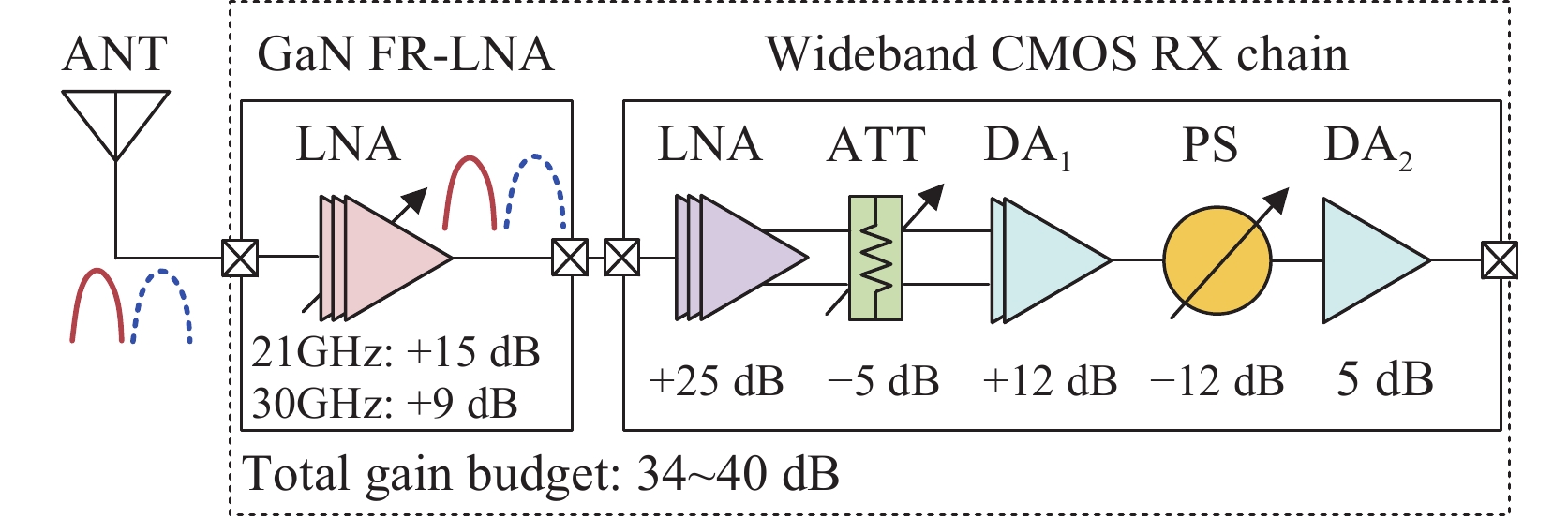
In this paper, a K/Ka-band frequency reconfigurable LNA (FR-LNA) is presented with a reconfigurable inter-stage and output matching network to be applied in a frequency reconfigurable hybrid phased array RX chain, as shown in Figure 1. The gain budget of the building blocks shows that the CMOS LNA needs to provide a gain of 25 dB. Two additional driver amplifiers, DA1 and DA2, are employed to compensate for the passive losses induced by the passive phase shifter and attenuator. The proposed FR-LNA can be reconfigured to operate at two frequency bands. Together with the wideband CMOS IC, the overall receiver can be applied for various scenarios, i.e., 5G NTN. A switch-based reconfigurable resonator (SBRR) is employed in both the inter-stage and output stage matching network of the FR-LNA, enabling frequency band switching. The utilization of reconfigurable components is straightforward to implement and features a simple structure, thus resulting in a compact chip size.
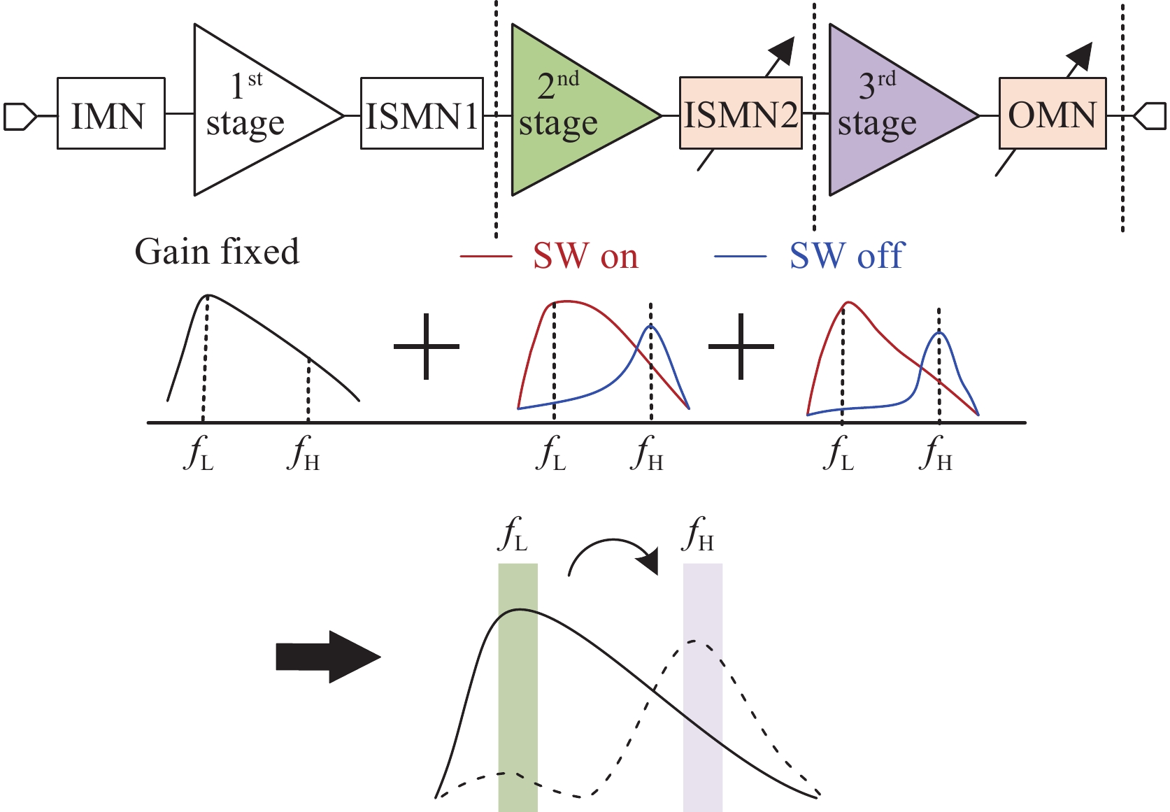
Figure 2 shows the design concept of the proposed FR-LNA, which consists of three amplification stages with reconfigurable inter-stage and output stages. The LNA is implemented in a commercial 0.15-μm GaN HEMT process with an fT of approximately 34.5 GHz.
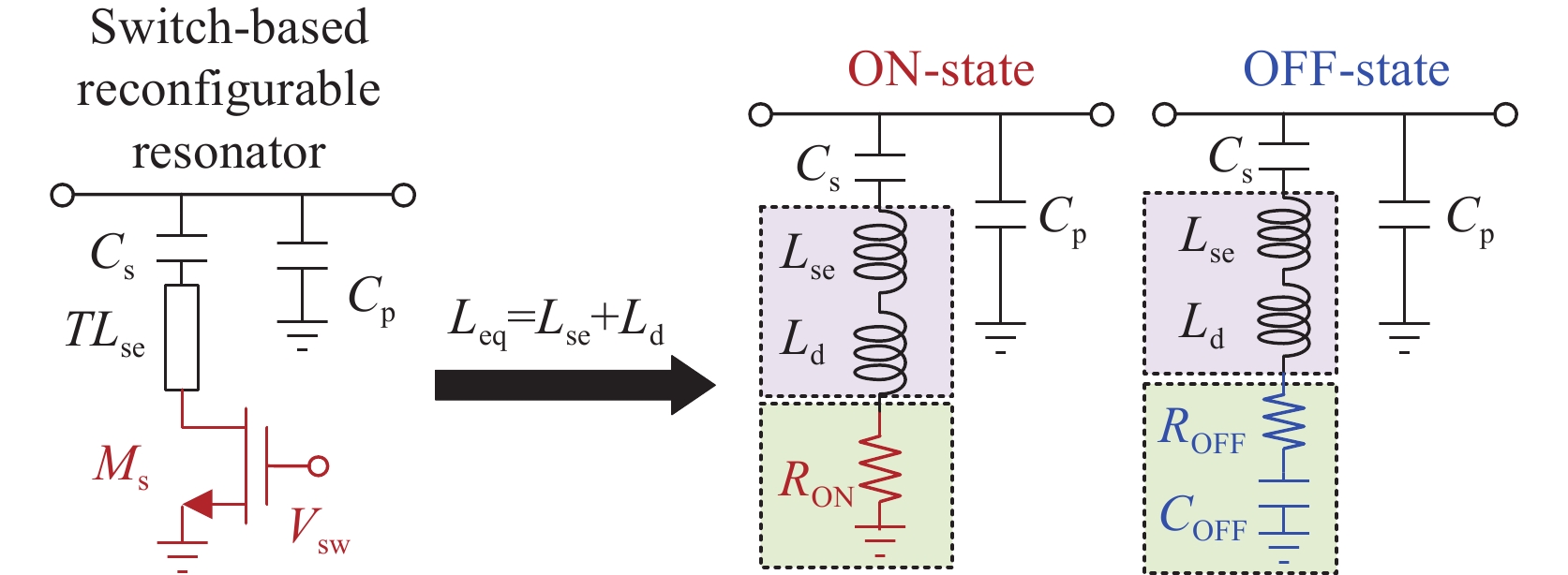
As depicted in Figure 3, the equivalent circuit of a GaN HEMT switch at ON- and OFF-state can be modeled by lumped series RLC circuit [22]–[24]. In contrast to the conventional circuit model for switch devices in the low-frequency band, a series inductor is included to model the parasitic effects of interconnect metals at high frequencies, particularly in millimeter-wave bands. This addition is crucial as it can significantly impact the RF performance of the switch in terms of insertion loss (IL) and isolation (ISO), making it imperative not to overlook. Nevertheless, when a switch HEMT is employed to achieve switchable or reconfigurable reactance by integrating capacitors and inductors, the parasitic parameters of the switch can be harnessed rather than eliminated through additional circuitry. This strategy serves to simplify the overall circuit complexity.
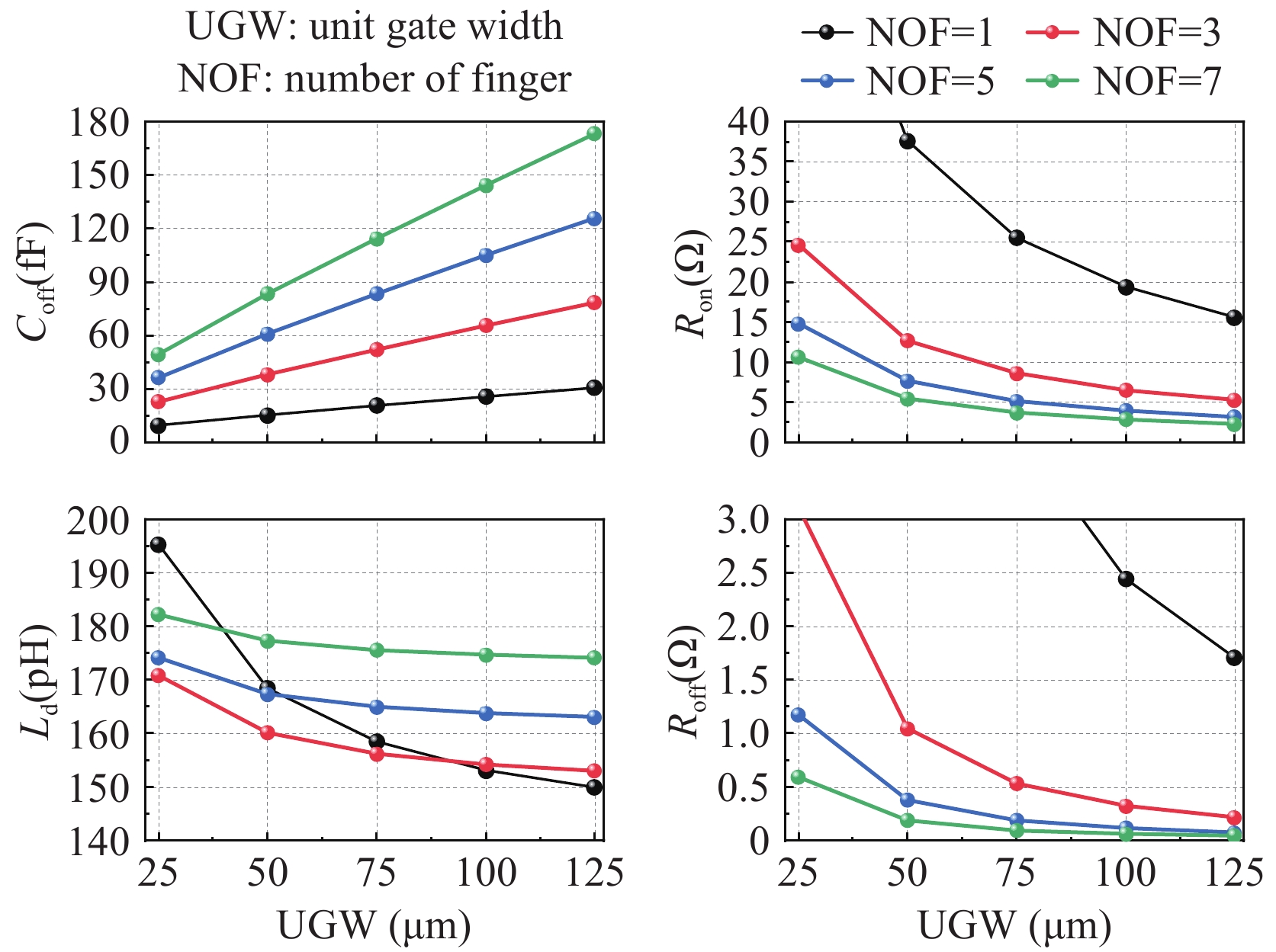
Figure 4 illustrates the RLC circuit parameters of the HEMT switch extracted at 30 GHz for different values of the unit gate width (UGW) and the number of fingers. The gate bias voltage is set to 0 V and −10 V for turning on and turning off, respectively, using a 5-kΩ bias resistor. The OFF-state capacitance (COFF) of the HEMT switch increases linearly with the gate width, whereas the ON-state resistance (RON) exhibits an opposite trend as the gate width increases. The OFF-state resistance (ROFF) can be considered negligible. The amount of parasitic inductance (Ld) remains relatively consistent at a given NOF. This consistency can be observed in Figure 2, where the primary contributor to parasitic inductance is the metal interconnection between the electrode’s PAD and the surrounding device.
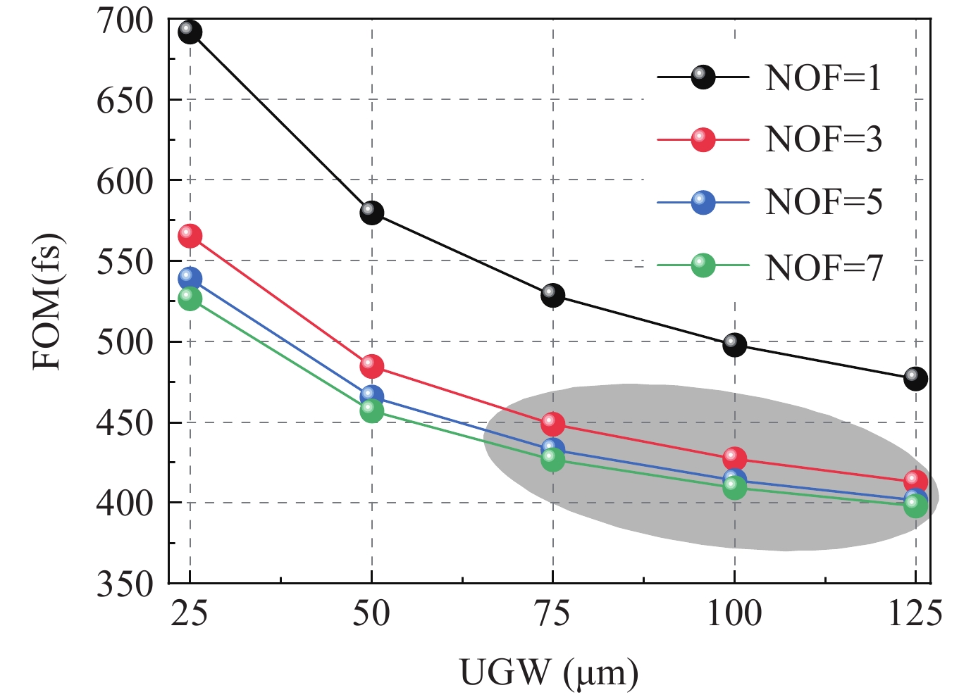
The size of this interconnecting metal remains largely uniform when the NOF is unchanged. The figure of merit (FOM) can be derived from the product of RON × COFF, with a typical value ranging from 400 to 700 fs, as shown in Figure 5. In addition, the optimal circuit parameter region of the switch is highlighted in gray.
Switch HEMT can manipulate the reactance of capac-itors or inductors by leveraging its distinct impedance in the ON- and OFF-states. This capability allows for the modification of the resonant frequency of LC resonators. The schematic of proposed SBRR network is depicted in Figure 6, where the HEMT switch Ms is connected in series with Cs and TLse to create transmission zeros, en-suring rejection of unwanted signals in the lower out-of-band region while exhibiting inductance within the operating frequency band. The series resonant frequency in the ON-state (fTZ1) and OFF-state (fTZ2) are given by (1) and (2), respectively,
| fTZ1=12π√LeqCs | (1) |
| fTZ2=12π√LeqCsCoff(Cs+Coff) | (2) |
where Leq is the sum of the parasitic inductance Ld of Ms and the extracted inductance Lse of transmission line TLse. The input admittance Yin of the SBRR can be calculated as (3), where Rsw is the parasitc resistance of switch (i.e., RON and ROFF), and fTZ is the transmission zero (i.e., fTZ1 and fTZ2).
| Yin=RswR2sw+2π(fLeq−f2TZLeq/f)2+jωCp+j⋅4π2Leq(f2TZ−f2)R2sw+2π(fLeq−f2TZLeq/f)2 | (3) |
Accordingly, the resonant frequency of the entire SBRR in the ON-state (fL) and OFF-state ((fH)) could also be deduced as (4) and (5).
| fL=12π√(1+4π2LeqCpf2TZ1)LeqCp | (4) |
| fH=12π√(1+4π2LeqCpf2TZ2)LeqCp | (5) |
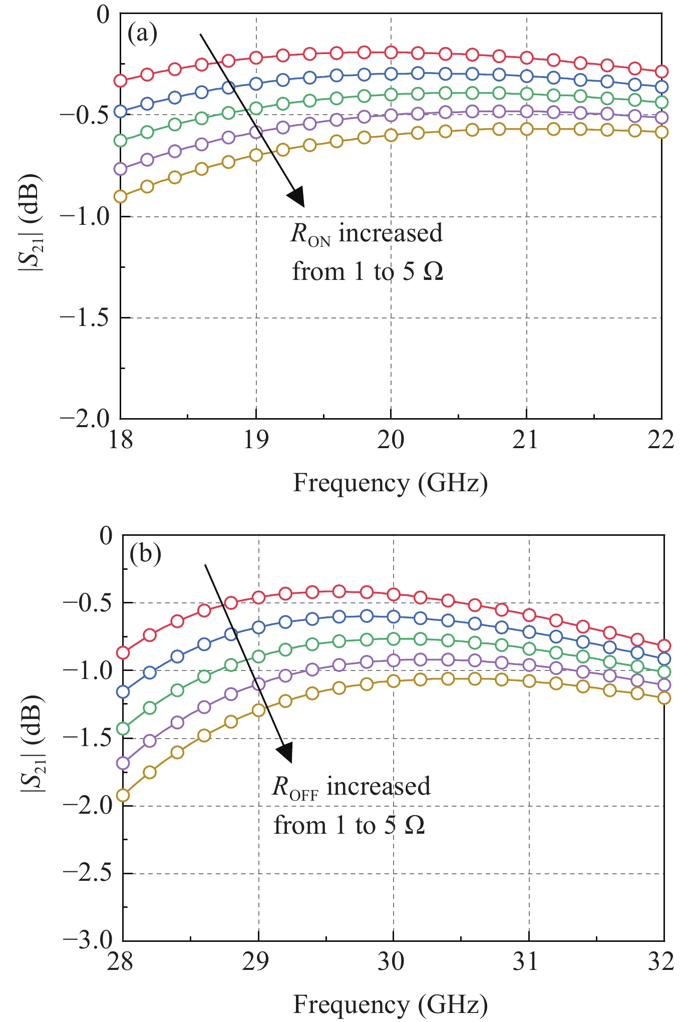
Figure 7 illustrates the simulated responses of the proposed SBRR at both states with a 5×100 μm HEMT. Moreover, extra IL can be induced by the parasitic resistances, with Ld=163.8 pH, COFF=105 fF, the IL of SBRR under different sets of RON and ROFF is shown in Figure 8(a) and Figure 8(b) with 50 Ω terminated. As can be seen, a low RON is crucial to reduce the IL. As the compromise of the RON and COFF discussed in Section 2, a switch HEMT size of 5×100 μm with a FOM of 414 fs is chosen in this design. The values of RON, ROFF, COFF and Ld are extracted to be 3.94 Ω, 0.116 Ω, 105 fF and 163.8 pH, respectively. Subsequently, the remaining components of the resonator are tuned to achieve the desired resonant frequency according to equation (1) − (5). By applying gate bias voltages of 0 V and −10 V, the resonant frequency reconfigured from 21 GHz to 30 GHz. The simulated out-of-band rejection in the higher frequency band is approximately −28 dBc around 25 GHz, which surpasses the rejection seen around 10 GHz in the lower frequency band. This is attributed to the low resistance when the switch is biased in the OFF-state, leading to a higher Q value of the resonator.
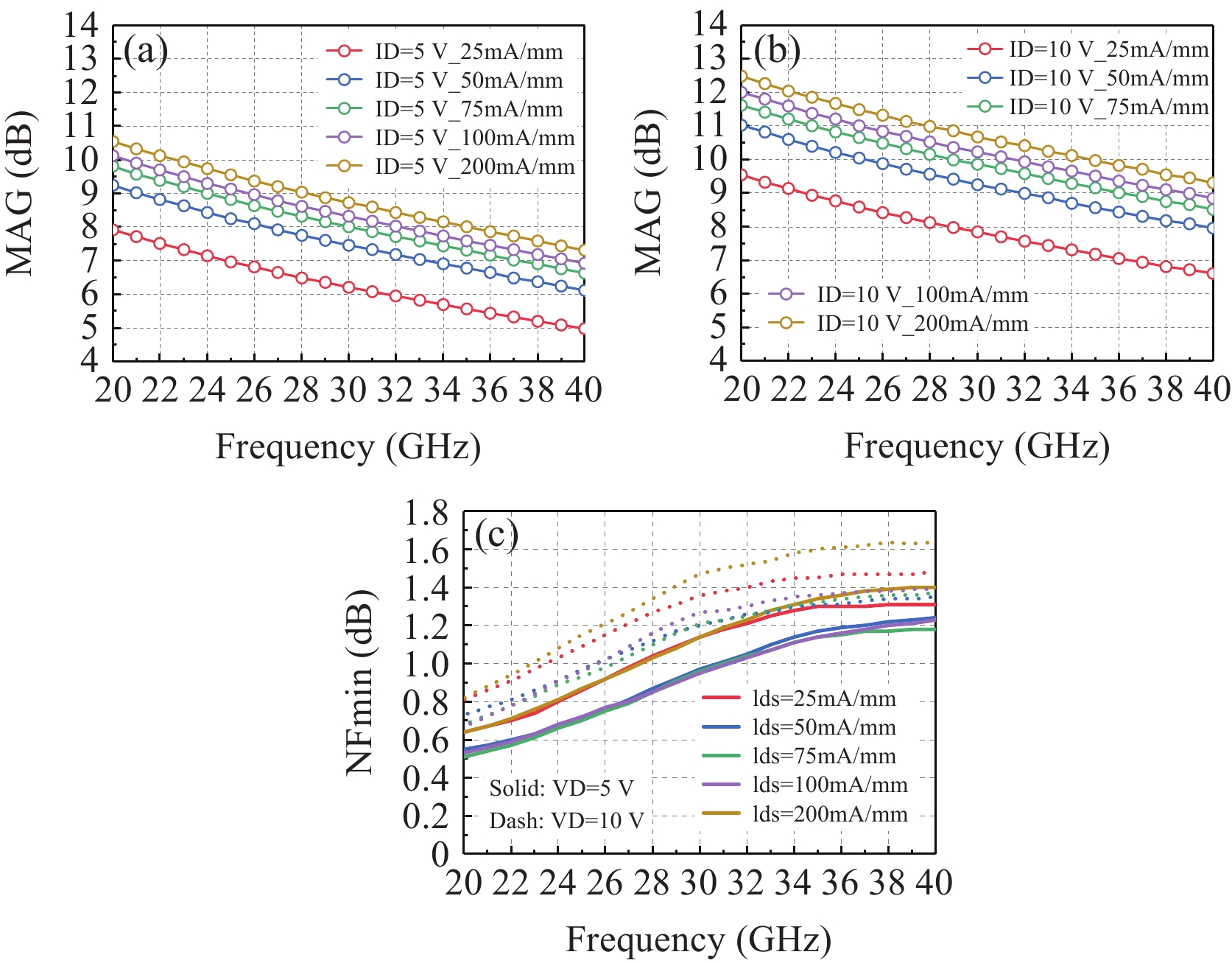
To obtain optimal NF and maximum available gain (MAG), the size of each HEMT is chosen to be 2×50 μm. In Figure 9, the MAG and noise figure minimum (NFmin) characteristics of a 2×50 μm common-source HEMT are depicted. In consideration of the MAG and NFmin, the quiescent current has been set at 100 mA/mm with a 5 V drain supply. A source-degenerated inductor of 134 pH is connected in series with the HEMT. Subsequently, the noise contour for the input stage at 21 GHz and 30 GHz is de-picted in Figure 10(a). The impedance of NFmin at 21 GHz and 30 GHz is 22.872 + j45.7 Ω and 15.9 + j16.8 Ω, re-spectively, with NFmin values of 0.57 dB and 1 dB. However, achieving optimal noise impedance matching simultaneously is challenging. Therefore, a simple high-pass matching network is selected to minimize IL. The impedance trajectory of the input matching network (IMN) is positioned at the plane of symmetry of the noise circle at 21 GHz and 30 GHz. By sacrificing a small amount of NF at the edges of the frequency band, the optimal NF is achieved at the mid-frequency, as shown in Figure 10(b). Nevertheless, the 1.07 dB and 1.38 dB NF at the two target frequencies of the input stage are still acceptable.
After determining the IMN, the output impedance of the first stage can be obtained. The value of the degenerated inductor in the second stage is 88.4 pH, which is smaller than that of the first stage to improve the overall gain of the LNA. The first inter-stage matching network (ISMN) is initially designed to transform the output impedance (Zd1) of the pre-stage to the optimal source impedance of the post-stage (Zs,opt2) at 21 and 30 GHz simultaneously.
To this end, a second-order bandpass network is considered with resistive load termination. Then, Zd1 is modeled as a parallel RC network, with the capacitor Cd1 integrated into the bandpass network. The optimal source impedance for the post-stage is represented by a series RC model. Additionally, an extra inductor (L3) is connected in parallel with the gate of the post-stage HEMT and in series with Cs. This configuration forms a high-pass network, transforming the impedance (Zim) into the optimal impedance (Zs,opt2). The ISMN1 is illustrated in Figure 11(a). To facilitate the implementation of component values on-chip, a Norton transformation is applied to the inductors in the band-pass network, resulting in a T-type network that simplifies the bias network. The simulated |S21| of the ISMN1 is depicted in Figure 11(b), along with the source impedance trajectory of the second stage. Figure 12(a) shows the proposed and the switch-based reconfigurable ISMN2, both terminated with the same impedance for performance comparison. The proposed ISMN2 comprises a second-order bandpass network and a high-order high-pass network for impedance transformation. This arrangement obviates the need for impedance scaling using Norton transformation, as the high-order high-pass network facilitates an effective transition from a high-impedance to a low-impedance region. The proposed SBRR is integrated into the bandpass network, as previously discussed. The transmission zero shifts with the gate control voltage of the switch HEMT, thereby reconfiguring the passband. It is evident that the operation frequency transitions to a high-band (HB) with the switch HEMT turned off, achieving significant rejection in the low-band (LB). The simulated |S21| of the proposed and switch-based ISMN2 is illustrated in Figure 12(b). The insertion loss of the switch-based solution outperforms that of the proposed SBRR method when the same switch device is used. However, regarding out-of-band rejection, the proposed SBRR exhibits superior rejection at lower frequencies in HB mode, attributed to the detrimental parasitic effects of the embedded switch device.
A reconfigurable output matching network (OMN) is designed with the proposed SBRR and is compared with a switch-based solution, as depicted in Figure 13(a). Due to the slightly higher Q value (8.7) at the lower band, a transformed second-order bandpass network, complemented by additional matching elements, has been adopted. The SBRR is integrated into the bandpass network, analogous to ISMN2. The parallel RC network, consisting of Rd3 and Cd3, can be derived from the output impedance of the third stage. The simulated |S21| of the proposed and switch-based OMN is illustrated in Figure 13(b). Similar to ISMN2, the proposed OMN exhibits superior rejection at lower frequencies in HB mode compared to the switch-based solution. The IL in LB mode is slightly greater than in HB mode, primarily attributed to the RON of the switch, as discussed in Section II.
The complete schematic of the proposed FR-LNA is illustrated in Figure 14. All the inductors in the above impedance matching network are realized using transmission lines (TLs). The width of each TL is 20 μm. TL3, TL8 and TL13 are utilized to realize inductive source degeneration, which facilitates impedance matching and ensure stable conditions.
The proposed SBRR is implemented in both the second inter-stage and output matching network, capacitors Cs1, Cs2, Cp1, and Cp2 are finely tuned to satisfy the matching condition. The gate and drain bias TLs are involved in impedance matching networks for a compact layout. The simulated gain of individual stages and the total LNA stages in the LB and HB modes are plotted in Figure 15(a) and Figure 15(b), respectively. Consequently, the operating frequency band of the proposed FR-LNA can be reconfigured by applying various control voltages. Moreover, transmission zeros are clearly observed in the lower out-of-band.
In [15], the switched input match is adopted to reconfigure the operating frequency band, but due to the limitations of switch FOM, it leads to increased IL, resulting in NF degradation. Moreover, the switched degenerated inductor further degrades NF. In [16], similarly to [15], a substrate-shielded inductor (SSI), utilizing a switch to reconfigure the reactance, is employed in the input matching network, which also contributes to NF degradation. The proposed SBRR in this design is integrated in the ISMN and OMN. Compared to the reconfigurable methods in [15] and [16], the proposed SBRR has minimal impact on the NF after the operating band is reconfigured, with only some reduction in gain resulting from the additional switch loss.
The micrograph of fabricated chip is shown in Figure 16. On-wafer measurements are conducted using GSG probes for RF input/output and DC probes for bias and power supply. The RF characterization setup is calibrated using the short-open-load-through (SOLT) method on a Keysight PNA-X analyzer, while power calibration is performed using a power meter.
The FR-LNA is biased at VD = 5 V, Vg = −1.5 V. The measured and simulated S-parameters and NF of the FR-LNA are presented in Figure 17 and Figure 18. The LB mode at 21 GHz achieves a gain of 13.9 dB with a NF of 2.4 dB. In the HB mode at 30 GHz, the FR-LNA obtains a gain of 8.9 dB with a NF of 3.2 dB. The out-of-band rejection exceeds 63 dBc at 16 GHz and 18 dBc at 20 GHz for LB and HB modes, respectively. It features excellent rejection against unwanted low-frequency signals, particularly for X-band satellite communications.
Furthermore, the output 1-dB compression point (OP1dB) of 5.4 and 6.7 dBm are achieved for the LB and HB modes, as illustrated in Figure 17(c) and Figure 18(c). In addition, the input-referred intercept point (IIP3) of the LNA is measured using a two-tone signal with 100 MHz tone spacing, as shown in Figure 19. The measured IIP3 is 2.56 dBm and 14.77 dBm at 21 GHz and 30 GHz, respectively, implying a good dynamic range for the receivers. The total power consumption (PDC) of the FR-LNA is approximately 210 mW.
The measured and simulated results reveal a close agreement. However, in LB mode, there are some discrepancies between simulation and measured S-parameters. As discussed in Section II, the parasitic parameters of switch device affect the performance of the SBRR, thus the overall performance of the LNA. The variation in fL and fH is may attributed to deviations in Ld and COFF between the model and the actual device. After Cs and Cp are determined, only the parasitic parameters of switch device affect the tow resonant frequencies, fL and fH. Specifically, in HB mode, the switch HEMT is turned off. If we assume that the value of Ld becomes smaller and COFF becomes larger than simulated values, these opposing variations may cancel each other out, causing the measured S-parameters to appear closer to the simulated results. Figure 20 shows the simulated |S21| of the FR-LNA with various Ld and COFF under HB and LB modes. As shown in Figure 20(a), the response of the LNA exhibits slight variation and remains close to the measured results. However, when it is reconfigured in LB mode (see Figure 20(b)), as the switch turned on, varying Ld prominently shifts the frequency response. Therefore, the discrepancies between simulated and measured results in LB mode become more pronounced. Besides, the discrepancy in the magnitude of S21 may be caused by a larger RON than the PDK model (see Figure 20(c)).
Table 1 summarizes the performance of the proposed FR-LNA and compares with prior works. Since few III-V reconfigurable LNAs demonstrated at K/Ka-band, the proposed FR-LNA is also compared with some wideband designs. Two figure-of-merits (FOMs) are calculated to evaluate the performance, including bandwidth, gain, NF, IP1dB, and PDC, as described in [25]:
| Ref. | [4] | [5] | [8] | [16] | [20] | This work |
| Tech. | 0.15-μm GaN | 0.15-μm GaN | 0.1-μm GaN | 65-nm CMOS | 0.1-μm GaAs | 0.15-μm GaN |
| Topology | wideband | wideband | wideband | reconfigurable | switchable | reconfigurable |
| Freq. (GHz) | 28 | 36 | 37 | 28/39 | 28/39 | 21/30 |
| BW (GHz) | 6 | 2 | 38 | 9/16 | 4.6/3 | 4.15/3 |
| Gain (dB) | 25a | 19.7 | 16–21.5 | 17.2/12.1 | 25.1/27.7 | 13.9/8.9 |
| NF (dB) | 2.4–2.9 | 3.7 | 2.2–4.4 | 2.8/4.4 | 2.4/2.8 | 2.4/3.2 |
| IP1dB (dBm) | −0.9b | 4.0b | −5 to -0.5 | −13.6/−11 | −18.3/−17 | −7.4b/−1.2b |
| IIP3(dBm) | 7.2a | N.A. | N.A. | −4/−2 | −8.8/−8.5 | 2.56/14.77 |
| OP1dB (dBm) | 19.1 | 22.7 | 10–20 | 2.6b/0.1b | 6.8b/10.7b | 5.5/6.7 |
| PDC (mW) | 300 | 28.5 | 74 | 210 | ||
| Area (mm2) | 3 | 5.2 | 4.8 | 0.157 | 1.6 | 2.625 |
| FOMD (dB) | −10.6 | −19.67 | −16.98 | −15.22/−18.7 | −14.06/−13.16 | −16.06/−17.4 |
| FOMDBW (dB) | −8 | −18.67 | −11.71 | −12/−14.69 | −11.85/−11.57 | −14/−15.8 |
| [a] Graphically estimated. [b] Calculated with OP1dB = IP1dB + Gain − 1. [c] Simulated results. | ||||||
 DownLoad:
CSV
DownLoad:
CSV
| FOMD=L×IP1dB×(G−1)×f1/30F−11−G−1×P2/3DC | (6) |
| FOMBWD=L×IP1dB×(G−1)×f2/30×(Δf/f0)1/3F−11−G−1×P2/3DC | (7) |
where L represents the gate length in μm, f0 is the center frequency in GHz, Δf is the bandwidth in GHz, IP1dB is in mW, G is the linear value of gain, and F is the noise factor. The proposed GaN FR-LNA showcases reconfigurable frequency capability and demonstrates comparable FOMs to its CMOS and GaAs counterparts, demonstrating its potential for multi-band communication systems.
This work is supported in part by the Guangdong Province Key Project of Science and Technology under grant 2020B010171002, in part by the National Natural Science Foundation of China (NSFC) under Grant
| [1] |
Y. Wang, D. You, X. Fu, et al., “A Ka-band SATCOM transceiver in 65-nm CMOS with high-linearity TX and dual-channel wide-dynamic-range RX for terrestrial terminal,” IEEE Journal of Solid-State Circuits, vol. 57, no. 2, pp. 356–370, 2022. DOI: 10.1109/JSSC.2021.3096190
|
| [2] |
A. S. Youssouf, M. H. Habaebi, and N. F. Hasbullah, “The radiation effect on low noise amplifier implemented in the space-aerial-terrestrial integrated 5G networks,” IEEE Access, vol. 9, pp. 46641–46651, 2021. DOI: 10.1109/ACCESS.2021.3065497
|
| [3] |
A. Kawaguchi, J. Pang, Z. Li, et al., “Total ionizing dose effects on 28GHz CMOS bi-directional transceiver for 5g non-terrestrial networks,” in Proceedings of 2020 20th European Conference on Radiation and its Effects on Components and Systems (RADECS), Toulouse, France, pp. 1–4, 2020.
|
| [4] |
H. B. Ahn, H. G. Ji, Y. Choi, et al., “25–31 GHz GAN-based LNA MMIC employing hybrid-matching topology for 5g base station applications,” IEEE Microwave and Wireless Technology Letters, vol. 33, no. 1, pp. 47–50, 2023. DOI: 10.1109/LMWC.2022.3201075
|
| [5] |
N. Nguyen, K. Phan, S. Lee, et al., “A 35–37 GHz MMIC GAN low noise amplifier,” in Proceedings of 2021 International Symposium on Electrical and Electronics Engineering (ISEE), Ho Chi Minh, Vietnam, pp. 26–29, 2021.
|
| [6] |
Z. J. Wang, D. B. Hou, Z. K. Li, et al., “A linearity-enhanced 18.7–36.5-GHz LNA with 1.5–2.1-db NF for radar applications,” IEEE Microwave and Wireless Components Letters, vol. 32, no. 8, pp. 972–975, 2022. DOI: 10.1109/LMWC.2022.3165124
|
| [7] |
Y. L. Hu and T. Y. Chi, “A 27–46-GHz low-noise amplifier with dual-resonant input matching and a transformer-based broadband output network,” IEEE Microwave and Wireless Components Letters, vol. 31, no. 6, pp. 725–728, 2021. DOI: 10.1109/LMWC.2021.3059592
|
| [8] |
X. D. Tong, L. Zhang, P. H. Zheng, et al., “An 18–56-GHz wideband GaN low-noise amplifier with 2.2–4.4-db noise figure,” IEEE Microwave and Wireless Components Letters, vol. 30, no. 12, pp. 1153–1156, 2020. DOI: 10.1109/LMWC.2020.3028311
|
| [9] |
Z. J. Wang, D. B. Hou, and W. Hong, “A pHEMT switch based dual-band switchable LNA for 5G millimeter-wave applications,” in Proceedings of 2022 15th UK-Europe-China Workshop on Millimetre-Waves and Terahertz Technologies (UCMMT), Tønsberg, Norway, pp. 1–4, 2021.
|
| [10] |
J. R. Fu, M. G. Bardeh, J. Paramesh, et al., “A millimeter-wave concurrent LNA in 22-nm CMOS FDSOI for 5G applications,” IEEE Transactions on Microwave Theory and Techniques, vol. 71, no. 3, pp. 1031–1043, 2023. DOI: 10.1109/TMTT.2022.3219869
|
| [11] |
D. Lee and C. Nguyen, “Dual Q/V-band SiGe BiCMOS low noise amplifiers using Q-enhanced metamaterial transmission lines,” IEEE Transactions on Circuits and Systems II: Express Briefs, vol. 68, no. 3, pp. 898–902, 2021. DOI: 10.1109/TCSII.2020.3020575
|
| [12] |
J. Lee and C. Nguyen, “A concurrent tri-band low-noise amplifier with a novel tri-band load resonator employing feedback notches,” IEEE Transactions on Microwave Theory and Techniques, vol. 61, no. 12, pp. 4195–4208, 2013. DOI: 10.1109/TMTT.2013.2288592
|
| [13] |
J. Y. Liu, S. B. Liu, Y. N. Gao, et al., “A 28-/39-GHz dual-band CMOS LNA with shunt-series transformer feedback,” IEEE Microwave and Wireless Technology Letters, vol. 33, no. 1, pp. 51–54, 2023. DOI: 10.1109/LMWC.2022.3201087
|
| [14] |
A. A. Nawaz, J. D. Albrecht, and A. Ç. Ulusoy, “A Ka/V band-switchable LNA with 2.8/3.4 dB noise figure,” IEEE Microwave and Wireless Components Letters, vol. 29, no. 10, pp. 662–664, 2019. DOI: 10.1109/LMWC.2019.2939540
|
| [15] |
K. W. Kobayashi, V. Kumar, C. Campbell, et al., “Robust-5W reconfigurable S/X-band GAN LNA using a 90nm T-gate GaN HEMT technology,” in Proceedings of 2020 IEEE BiCMOS and Compound Semiconductor Integrated Circuits and Technology Symposium (BCICTS), Monterey, CA, USA, pp. 1–4, 2021.
|
| [16] |
H. H. Chen and Z. M. Tsai, “Ka-/K-band frequency-reconfigurable single-input differential-output low-noise amplifier for 5G applications,” IEEE Microwave and Wireless Technology Letters, vol. 33, no. 9, pp. 1297–1300, 2023. DOI: 10.1109/LMWT.2023.3288625
|
| [17] |
S. N. Ali, M. A. Hoque, S. Gopal, et al., “A continually-stepped variable-gain LNA in 65-nm CMOS enabled by a tunable-transformer for mm-wave 5G communications,” in Proceedings of 2019 IEEE MTT-S International Microwave Symposium (IMS), Boston, MA, USA, pp. 926–929, 2019.
|
| [18] |
C. J. Liang, Y. Zhang, C. W. Chiang, et al., “A K/Ka/V triband single-signal-path receiver with variable-gain low-noise amplifier and constant-gain phase shifter in 28-nm CMOS,” IEEE Transactions on Microwave Theory and Techniques, vol. 69, no. 5, pp. 2579–2593, 2021. DOI: 10.1109/TMTT.2021.3061707
|
| [19] |
S. Lee and S. Hong, “Frequency-reconfigurable dual-band low-noise amplifier with interstage gm-boosting for millimeter-wave 5G communication,” IEEE Microwave and Wireless Technology Letters, vol. 33, no. 4, pp. 463–466, 2023. DOI: 10.1109/LMWT.2022.3220975
|
| [20] |
Z. J. Wang, D. B. Hou, P. G. Zhou, et al., “A Ka-band switchable LNA with 2.4-dB NF employing a varactor-based tunable network,” IEEE Microwave and Wireless Components Letters, vol. 31, no. 4, pp. 385–388, 2021. DOI: 10.1109/LMWC.2021.3059655
|
| [21] |
R. A. Shaheen, T. Rahkonen, and A. Pärssinen, “Millimeter-wave frequency reconfigurable low noise amplifiers for 5G,” IEEE Transactions on Circuits and Systems II: Express Briefs, vol. 68, no. 2, pp. 642–646, 2021. DOI: 10.1109/TCSII.2020.3014571
|
| [22] |
T. Kim, H. Im, S. H. Lee, et al., “Highly linear K-/Ka-band SPDT switch based on traveling-wave concept in a 150-nm GaN pHEMT process,” IEEE Microwave and Wireless Components Letters, vol. 32, no. 8, pp. 987–990, 2022. DOI: 10.1109/Lmwc.2022.3161498
|
| [23] |
G. X. Shen, W. Q. Che, H. S. Zhu, et al., “Analytical design of millimeter-wave 100-nm GaN-on-Si MMIC switches using FET-based resonators and coupling matrix method,” IEEE Transactions on Microwave Theory and Techniques, vol. 69, no. 7, pp. 3307–3318, 2021. DOI: 10.1109/TMTT.2021.3081113
|
| [24] |
G. X. Shen, H. S. Zhu, Q. Cai, et al., “Compact multipole GaN-on-Si SPDT switch using inductive parasitic effects of hybrid HEMT devices,” IEEE Transactions on Microwave Theory and Techniques, vol. 71, no. 11, pp. 4778–4786, 2023. DOI: 10.1109/TMTT.2023.3267543
|
| [25] |
L. Belostotski and E. A. M. Klumperink, “Figures of merit for CMOS low-noise amplifiers and estimates for their theoretical limits,” IEEE Transactions on Circuits and Systems II: Express Briefs, vol. 69, no. 3, pp. 734–738, 2022. DOI: 10.1109/TCSII.2021.3113607
|
| [1] | WEI Shaojun, LU Yan'an. The Principle and Progress of Dynamically Reconfigurable Computing Technologies[J]. Chinese Journal of Electronics, 2020, 29(4): 595-607. DOI: 10.1049/cje.2020.05.002 |
| [2] | DUAN Tong, LAN Julong, HU Yuxiang, LIU Shiran. A Reconfigurable Hardware Architecture for Packet Processing[J]. Chinese Journal of Electronics, 2018, 27(2): 428-432. DOI: 10.1049/cje.2017.08.018 |
| [3] | LI Wei, ZENG Xiaoyang, DAI Zibin, NAN Longmei, CHEN Tao, MA Chao. A High Energy-Efficient Reconfigurable VLIW Symmetric Cryptographic Processor with Loop Buffer Structure and Chain Processing Mechanism[J]. Chinese Journal of Electronics, 2017, 26(6): 1161-1167. DOI: 10.1049/cje.2017.06.010 |
| [4] | GUO Qi, WANG Long, SHEN Shuting. Multiple-Channel Local Binary Fitting Model for Medical Image Segmentation[J]. Chinese Journal of Electronics, 2015, 24(4): 802-806. DOI: 10.1049/cje.2015.10.023 |
| [5] | SHAN Weiwei, CHEN Xin, LU Yinchao, LI Jie. A Novel Combinatorics-Based Reconfigurable Bit Permutation Network and Its Circuit Implementation[J]. Chinese Journal of Electronics, 2015, 24(3): 513-517. DOI: 10.1049/cje.2015.07.013 |
| [6] | WANG Xue, QIAN Zhihong, SUN Dayang. A Uniqueness Guarantee Timing Synchronization Algorithm for MB-OFDM Based UWB Systems[J]. Chinese Journal of Electronics, 2013, 22(1): 141-145. |
| [7] | HONG Qi, CAO Wei, TONG Jiarong. A Dynamically Reconfigurable VLSI Architecture for H.264 Integer Transforms[J]. Chinese Journal of Electronics, 2012, 21(3): 510-514. |
| [8] | CHEN Ming. Optimum Design of Multi-band Transformer with Multi-section for Two Arbitrary Complex Frequency-dependent Impedances[J]. Chinese Journal of Electronics, 2012, 21(1): 160-164. |
| [9] | ZHANG Bowei, GU Guochang, SUN Lin, WU Yanxia. Floating-Point FPGA Gaussian Elimination in Reconfigurable Computing System[J]. Chinese Journal of Electronics, 2011, 20(1): 51-54. |
| [10] | Wu Xiaochun, Wu Chunming, Jia Fenggen. Research on a Synchronization Algorithm of Look-up Table in Open Reconfigurable Router[J]. Chinese Journal of Electronics, 2010, 19(3): 419-422. |
Figures(20) / Tables(1)

CJE QR CODE

CIE QR CODE
Copyright © Editorial Office of Chinese Journal of Electronics |
京ICP备12041980号-1 |

| Ref. | [4] | [5] | [8] | [16] | [20] | This work |
| Tech. | 0.15-μm GaN | 0.15-μm GaN | 0.1-μm GaN | 65-nm CMOS | 0.1-μm GaAs | 0.15-μm GaN |
| Topology | wideband | wideband | wideband | reconfigurable | switchable | reconfigurable |
| Freq. (GHz) | 28 | 36 | 37 | 28/39 | 28/39 | 21/30 |
| BW (GHz) | 6 | 2 | 38 | 9/16 | 4.6/3 | 4.15/3 |
| Gain (dB) | 25a | 19.7 | 16–21.5 | 17.2/12.1 | 25.1/27.7 | 13.9/8.9 |
| NF (dB) | 2.4–2.9 | 3.7 | 2.2–4.4 | 2.8/4.4 | 2.4/2.8 | 2.4/3.2 |
| IP1dB (dBm) | −0.9b | 4.0b | −5 to -0.5 | −13.6/−11 | −18.3/−17 | −7.4b/−1.2b |
| IIP3(dBm) | 7.2a | N.A. | N.A. | −4/−2 | −8.8/−8.5 | 2.56/14.77 |
| OP1dB (dBm) | 19.1 | 22.7 | 10–20 | 2.6b/0.1b | 6.8b/10.7b | 5.5/6.7 |
| PDC (mW) | 300 | 28.5 | 74 | 210 | ||
| Area (mm2) | 3 | 5.2 | 4.8 | 0.157 | 1.6 | 2.625 |
| FOMD (dB) | −10.6 | −19.67 | −16.98 | −15.22/−18.7 | −14.06/−13.16 | −16.06/−17.4 |
| FOMDBW (dB) | −8 | −18.67 | −11.71 | −12/−14.69 | −11.85/−11.57 | −14/−15.8 |
| [a] Graphically estimated. [b] Calculated with OP1dB = IP1dB + Gain − 1. [c] Simulated results. | ||||||
DownLoad:
CSV